COA Tutorial
Basic CO and Design
Computer Instructions
Digital Logic Circuits
Map Simplification
Combinational Circuits
Flip - Flops
Digital Components
Register Transfer
Micro-Operations
Memory Organization
COA_Misc
- Booth's Multiplication Algorithm
- Branch Instruction in Computer Organization
- Data Representation in Computer Organization
- ALU and Data Path in Computer Organization
- External memory in Computer Organization
- Structured Computer Organization
- Types of Register in Computer Organization
- Secondary Storage Devices in Computer Organization
- Types of Operands in Computer Organization
- Serial Communication in Computer organization
- Addressing Sequencing in Computer Organization
- Simplified Instructional Computer (SIC)
- Arithmetic Instructions in AVR microcontroller
- Conventional Computing VS Quantum Computing
- Instruction set used in Simplified Instructional Computer
- Branch Instruction in AVR microcontroller
- Conditional Branch instruction in AVR Microcontroller
- Data transfer instruction in AVR microcontroller
- Difference between Memory-based and Register-based addressing modes
- Difference between 1's complement Representation and 2's complement Representation
- CALL Instructions and Stack in AVR Microcontroller
- Difference between Call and Jump Instructions
- Overflow in Arithmetic Addition in Binary number System
- Horizontal Micro-programmed Vs. Vertical Micro-programmed Control Unit
- Hardwired Vs. Micro-programmed Control Unit
- Non-Restoring Division Algorithm for Unsigned Integer
- Restoring Division Algorithm for Unsigned Integer
- Debugging a Machine-level Program
- Dependencies and Data Hazard in pipeline in Computer Organization
- Execution, Stages and Throughput in Pipeline
- Types of Pipeline Delay and Stalling
- Timing Diagram of MOV Instruction
- Advantages and Disadvantages of Flash Memory
- Importance/Need of negative feedback in amplifiers
- Anti-Aliasing - Computer Graphics
- Bus Arbitration in Computer Organization
- Convert a number from Base 2 (Binary) to Base 6
- Cache Coherence
- EHCI
- Cache Memory and Virtual Memory
- Electrical Potential and Potential Difference
- RAM and Cache
- SIM and RIM instructions in 8085 processor
- Clusters in Computer Organization
- Data Types and Addressing Modes of 80386/80386DX Microprocessor
Timing Diagram of MOV Instruction
In order to understand the timing diagram of MOV instruction, we have to first learn about the MOV instruction.
MOV Instruction:
The MOV instruction is used to copy the data of item, which is referred to as the second operand of the instruction (Constant value, register content, or memory content), into the location, which is referred to by its first operand (memory or register). In the MOV instruction, it is not possible to do direct memory to memory moves, but it is possible to do register to register moves. If there is some case in which memory transfers are desired, then the content of source memory will be first loaded into a register. After that, it can be stored in a destination memory address.
Syntax: The syntax of MOV instruction is described as follows:
- mov <reg>,<reg>
- mov <reg>,<const>
- mov <reg>,<mem>mov <mem>,<reg>
- mov <mem>,<const>
Problem: Here, we have an instruction given below, and we have to draw the timing diagram of that instruction.
- MOV B, C
The above instruction is used to copy the content of first register into the second register without changing the content of first or source register.
Example:
- MOV B, C
- Opcode: MOV
- Operand: B and C
Here B is used to indicate the destination register, and C is used to indicate the source register. In the above example, the content of C needs to be transferred into B.
Algorithm:
The above instruction MOV B, C only requires 1 byte. So we only require one memory address to store the instruction completely. For example:
- 2000: MOV B, C
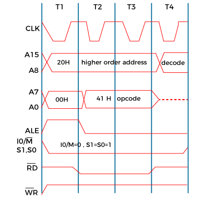
The above instruction needs the opcode fetching. So we can generate the timing diagram with the help of 4T states. For the opcode fetch, the IO/M (low active) = 0, S0 = 1, and S1 = 1.
Now we will draw the timing diagram of MOV instruction, which is described as follows:

In Opcode fetch (t1-t4 states):
00: It is used to indicate the lower bit of address in which opcode is stored.
20: It is used to indicate the higher bit of address in which opcode is stored.
ALE: It is used to send signals for data buses and multiplexed addresses. Only in t1, it will be used to fetch the lower bit of address with the help of address bus. In all the other cases, it will be used as a data bus.
RD (Low active): In t1 and t4, the signal is 1, which shows that none of the data is ready by a microprocessor. In t2 and t3, the signal is 0, which shows that the data is ready by a microprocessor.
WR (Low active): Here, the signal is 1 throughput which shows that none of the data is written with the help of a microprocessor.
IO/M (Low active): Here, the signal is 1 throughput which shows that the operation is performing on memory.
S0 and S1: If S0 and S1 try to fetch the opcode, then they will be 1.


