COA Tutorial
Basic CO and Design
Computer Instructions
Digital Logic Circuits
Map Simplification
Combinational Circuits
Flip - Flops
Digital Components
Register Transfer
Micro-Operations
Memory Organization
COA_Misc
- Booth's Multiplication Algorithm
- Branch Instruction in Computer Organization
- Data Representation in Computer Organization
- ALU and Data Path in Computer Organization
- External memory in Computer Organization
- Structured Computer Organization
- Types of Register in Computer Organization
- Secondary Storage Devices in Computer Organization
- Types of Operands in Computer Organization
- Serial Communication in Computer organization
- Addressing Sequencing in Computer Organization
- Simplified Instructional Computer (SIC)
- Arithmetic Instructions in AVR microcontroller
- Conventional Computing VS Quantum Computing
- Instruction set used in Simplified Instructional Computer
- Branch Instruction in AVR microcontroller
- Conditional Branch instruction in AVR Microcontroller
- Data transfer instruction in AVR microcontroller
- Difference between Memory-based and Register-based addressing modes
- Difference between 1's complement Representation and 2's complement Representation
- CALL Instructions and Stack in AVR Microcontroller
- Difference between Call and Jump Instructions
- Overflow in Arithmetic Addition in Binary number System
- Horizontal Micro-programmed Vs. Vertical Micro-programmed Control Unit
- Hardwired Vs. Micro-programmed Control Unit
- Non-Restoring Division Algorithm for Unsigned Integer
- Restoring Division Algorithm for Unsigned Integer
- Debugging a Machine-level Program
- Dependencies and Data Hazard in pipeline in Computer Organization
- Execution, Stages and Throughput in Pipeline
- Types of Pipeline Delay and Stalling
- Timing Diagram of MOV Instruction
- Advantages and Disadvantages of Flash Memory
- Importance/Need of negative feedback in amplifiers
- Anti-Aliasing - Computer Graphics
- Bus Arbitration in Computer Organization
- Convert a number from Base 2 (Binary) to Base 6
- Cache Coherence
- EHCI
- Cache Memory and Virtual Memory
- Electrical Potential and Potential Difference
- RAM and Cache
- SIM and RIM instructions in 8085 processor
- Clusters in Computer Organization
- Data Types and Addressing Modes of 80386/80386DX Microprocessor
Binary Adder
The Add micro-operation requires registers that can hold the data and the digital components that can perform the arithmetic addition.
A Binary Adder is a digital circuit that performs the arithmetic sum of two binary numbers provided with any length.
A Binary Adder is constructed using full-adder circuits connected in series, with the output carry from one full-adder connected to the input carry of the next full-adder.
The following block diagram shows the interconnections of four full-adder circuits to provide a 4-bit binary adder.
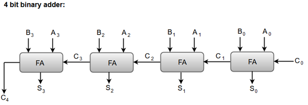
- The augend bits (A) and the addend bits (B) are designated by subscript numbers from right to left, with subscript '0' denoting the low-order bit.
- The carry inputs starts from C0 to C3 connected in a chain through the full-adders. C4 is the resultant output carry generated by the last full-adder circuit.
- The output carry from each full-adder is connected to the input carry of the next-high-order full-adder.
- The sum outputs (S0 to S3) generates the required arithmetic sum of augend and addend bits.
- The n data bits for the A and B inputs come from different source registers. For instance, data bits for A input comes from source register R1 and data bits for B input comes from source register R2.
- The arithmetic sum of the data inputs of A and B can be transferred to a third register or to one of the source registers (R1 or R2).