COA Tutorial
Basic CO and Design
Computer Instructions
Digital Logic Circuits
Map Simplification
Combinational Circuits
Flip - Flops
Digital Components
Register Transfer
Micro-Operations
Memory Organization
COA_Misc
- Booth's Multiplication Algorithm
- Branch Instruction in Computer Organization
- Data Representation in Computer Organization
- ALU and Data Path in Computer Organization
- External memory in Computer Organization
- Structured Computer Organization
- Types of Register in Computer Organization
- Secondary Storage Devices in Computer Organization
- Types of Operands in Computer Organization
- Serial Communication in Computer organization
- Addressing Sequencing in Computer Organization
- Simplified Instructional Computer (SIC)
- Arithmetic Instructions in AVR microcontroller
- Conventional Computing VS Quantum Computing
- Instruction set used in Simplified Instructional Computer
- Branch Instruction in AVR microcontroller
- Conditional Branch instruction in AVR Microcontroller
- Data transfer instruction in AVR microcontroller
- Difference between Memory-based and Register-based addressing modes
- Difference between 1's complement Representation and 2's complement Representation
- CALL Instructions and Stack in AVR Microcontroller
- Difference between Call and Jump Instructions
- Overflow in Arithmetic Addition in Binary number System
- Horizontal Micro-programmed Vs. Vertical Micro-programmed Control Unit
- Hardwired Vs. Micro-programmed Control Unit
- Non-Restoring Division Algorithm for Unsigned Integer
- Restoring Division Algorithm for Unsigned Integer
- Debugging a Machine-level Program
- Dependencies and Data Hazard in pipeline in Computer Organization
- Execution, Stages and Throughput in Pipeline
- Types of Pipeline Delay and Stalling
- Timing Diagram of MOV Instruction
- Advantages and Disadvantages of Flash Memory
- Importance/Need of negative feedback in amplifiers
- Anti-Aliasing - Computer Graphics
- Bus Arbitration in Computer Organization
- Convert a number from Base 2 (Binary) to Base 6
- Cache Coherence
- EHCI
- Cache Memory and Virtual Memory
- Electrical Potential and Potential Difference
- RAM and Cache
- SIM and RIM instructions in 8085 processor
- Clusters in Computer Organization
- Data Types and Addressing Modes of 80386/80386DX Microprocessor
Bus and Memory Transfers
A digital system composed of many registers, and paths must be provided to transfer information from one register to another. The number of wires connecting all of the registers will be excessive if separate lines are used between each register and all other registers in the system.
A bus structure, on the other hand, is more efficient for transferring information between registers in a multi-register configuration system.
A bus consists of a set of common lines, one for each bit of register, through which binary information is transferred one at a time. Control signals determine which register is selected by the bus during a particular register transfer.
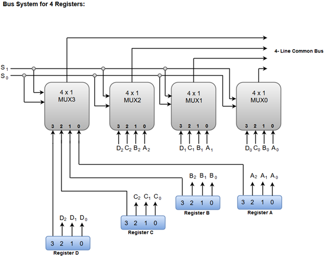
The following block diagram shows a Bus system for four registers. It is constructed with the help of four 4 * 1 Multiplexers each having four data inputs (0 through 3) and two selection inputs (S1 and S2).
We have used labels to make it more convenient for you to understand the input-output configuration of a Bus system for four registers. For instance, output 1 of register A is connected to input 0 of MUX1.

The two selection lines S1 and S2 are connected to the selection inputs of all four multiplexers. The selection lines choose the four bits of one register and transfer them into the four-line common bus.
When both of the select lines are at low logic, i.e. S1S0 = 00, the 0 data inputs of all four multiplexers are selected and applied to the outputs that forms the bus. This, in turn, causes the bus lines to receive the content of register A since the outputs of this register are connected to the 0 data inputs of the multiplexers.
Similarly, when S1S0 = 01, register B is selected, and the bus lines will receive the content provided by register B.
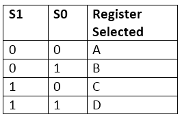
The following function table shows the register that is selected by the bus for each of the four possible binary values of the Selection lines.

Note: The number of multiplexers needed to construct the bus is equal to the number of bits in each register. The size of each multiplexer must be 'k * 1' since it multiplexes 'k' data lines. For instance, a common bus for eight registers of 16 bits each requires 16 multiplexers, one for each line in the bus. Each multiplexer must have eight data input lines and three selection lines to multiplex one significant bit in the eight registers.
A bus system can also be constructed using three-state gates instead of multiplexers.
The three state gates can be considered as a digital circuit that has three gates, two of which are signals equivalent to logic 1 and 0 as in a conventional gate. However, the third gate exhibits a high-impedance state.
The most commonly used three state gates in case of the bus system is a buffer gate.
The graphical symbol of a three-state buffer gate can be represented as:

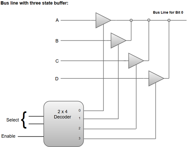
The following diagram demonstrates the construction of a bus system with three-state buffers.

- The outputs generated by the four buffers are connected to form a single bus line.
- Only one buffer can be in active state at a given point of time.
- The control inputs to the buffers determine which of the four normal inputs will communicate with the bus line.
- A 2 * 4 decoder ensures that no more than one control input is active at any given point of time.
Memory Transfer
Most of the standard notations used for specifying operations on memory transfer are stated below.
- The transfer of information from a memory unit to the user end is called a Read operation.
- The transfer of new information to be stored in the memory is called a Write operation.
- A memory word is designated by the letter M.
- We must specify the address of memory word while writing the memory transfer operations.
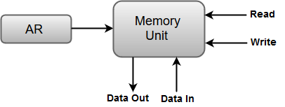
- The address register is designated by AR and the data register by DR.
- Thus, a read operation can be stated as:
- Read: DR ← M [AR]
- The Read statement causes a transfer of information into the data register (DR) from the memory word (M) selected by the address register (AR).
- And the corresponding write operation can be stated as:
- Write: M [AR] ← R1
- The Write statement causes a transfer of information from register R1 into the memory word (M) selected by address register (AR).


